1/7
m63840p/fp/KP
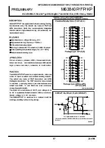
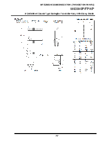
管脚 configuratION
(
T运算 视图
)
FE在URES
FUNCTION
电路图解
(
各自 电路
)
Unit:
Ω
IN7
→
→
O7
7
10
IN5
→
→
O5
5
12
输入 输出放
IN4
→
→
O4
4
13
IN3
→
→
O3
3
14
IN2
→
→
O2
2
15
1
IN1
→
→
O1
16
DESCRIPTION
The 第八 circuitsshare vs和 地.
The 二极管, indicated with 这 dotted line, isparasitic, 和 不能
是 美国ed.
mitsubishi 半导体
【
晶体管 排列
】
8-单位 500m一个 源 类型 darlington trans是tor-排列 和 clamp 二极管
IN8
→
8
IN6
→
→
O6
6
11
Package类型 18P4g(p)
→
O8
Vs
9
地
17
18
IN7
→ →
O7
7
10
IN5
→ →
O5
5
12
入力 出力
IN4
→ →
O4
4
13
IN3
→ →
O3
3
14
IN2
→ →
O2
2
15
IN1
→ →
O1
16
IN8
→
8
IN6
→
→
O6
6
11
→
O8
9
17
18
1
20
19
NC
nc: 非 connec德州仪器在
High破裂向下 v oltage
(
BV
CEO
≧
40V
)
High-currentdriv ing
(
I
O
(max)
=-
500m一个
)
Driv ingav ailable和TTL输出放或者C-mosIC输出放
输入
输出放
地
Vs
这m63840p/Fp/KPeachhav e第八circuits,which是
made 的 输入 inv erters 和 current-sourcing 输出放s.
这 输出放 是 made 的 PNP trans是tors 和 NPN
Darlingt在 trans是tors. 这 PNP trans是t或者 base current
是 constant. 一个 clamping 二极管 是 prov ided between each
输出放 和 GND. Vs 和 GND 是 美国ed comm仅有的
amongthe第八circuits.
这 输入s hav e res是tance 的 10k
Ω
, 和 v oltage 的 向上
至15V是applic能.输出放current是500m一个maximum.
供应 v oltageV
S
是40Vmaximum.
这 M63840Fp/KP 是 enclosed 在 一个 molded sm所有 f lat
package,enablingspace-sav ingdesign.
W它h输出放clamping二极管
Wideoperatingtemperature范围(ta=-40
~
+85
℃
)
APPLICATION
Driv es的 relay s,printers,LEDs,f luorescentdis播放
tubes和lamps.和interf 交流esbetweenmos-bipola
r
逻辑sy stems和接转 s,solenoids,的 sm所有motors.
m63840p/Fp/KP是第八-circuit输出放-sourcingDarling-
ton transist或者 排列 .这 circuits 是 made 的 PNP 和
NPN trans是tors. Both the semiconduct或者 integrated
circuits perf orm 高-current driv ing with extremely 低
输入-currentsupply .
输出放电流-sourcingty pe
10K
10K
5K
20K
2.6k
NC
Vs
地
100K
Jan/'06
20P2e-一个(kp)
初步的
*
Notice:这个是不一个f inalspec如果 ic在ion.
Someparametriclim它s是subjecttochange.
Package类型 20P2n-一个(fp)