www.德州仪器.com
产品 预告(展)
OPA277
DAC7811
I
OUT1
V
输出
15V
V+
V
−
−
15V
R
FB
地
V
DD
V
DD
V
REF
I
OUT2
SerialInterface
InputShiftRegister
DAC7811
SBAS337–APRIL2005
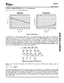
theoryofoperation(持续)
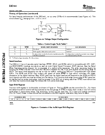
forbestlinearityperformanceofthedac7811,anopamp(opa277)isrecommended(seefigure26).这个
circuitallowsV
REF
swingingfrom–10vto+10v.
figure26.voltageoutputconfiguration
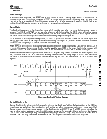
table2.controllogictruthtable
(1)
CLKSYNCSERIALSHIFTREGISTERDACREGISTER
XHNoeffectLatched
↑
+LShiftregisterdataadvancedonebitLatched
X
↑
+indaisy-chainmodethefunctionasdeterminedbyindaisy-chainmodethecontentsmaychage
c3-c0isexecuted.asdeterminedbyc3-c0.
(1)
↑
+
positivelogictransition;
X
=donotcare.
thedac7811hasathree-wireserialinterface(同步,sclk,andsdin),whichiscompatiblewithspi,qspi,
andmicrowireinterfacestandardsaswellasmostdigitalsignalprocessor(dsp)设备.seetheserial
writeoperationtimingdiagramforanexampleofatypicalwritesequence.thewritesequencebeginsby
bringingthesynclinelow.datafromthedinlineisclockedintothe16-bitshiftregisteronthefallingedgeof
sclk.theserialclockfrequencycanbeashighas50mhz,makingthedac7811compatiblewithhigh-速
dsps.thesdinandsclkinputbuffersaregatedoffwhilesyncishighwhichminimizesthepower
dissipationofthedigitalinterface.aftersyncgoeslow,thedigitalinterfacewillrespondtothesdinandsclk
inputsignalsanddatacannowbeshiftedintothedevice.ifaninactiveclockedgeoccursaftersyncgoeslow,
butbeforethefirstactiveclockedge,itwillbeignored.ifthesdopinisbeingusedthensyncmustremainlow
untilaftertheinactiveclockedgethatfollowsthe16thactiveclockedge.
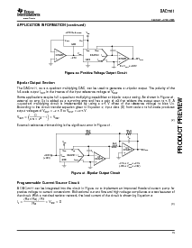
theinputshiftregisteris16bitswide,asshowninfigure27.thefourmsbsarethecontrolbitsc3–c0;这些
bitsdeterminewhichfunctionwillbeexecutedattherisingedgeofsyncindaisy-chainmodeorthe16thactive
clockedgeinstand-alonemode.theremaining12bitsarethedatabits.onaloadandupdatecommand
(c3–c0=0001)these12databitswillbetransferredtothedacregister;否则,theyhavenoeffect.
4CONTROLBITS12DATABITS
C3C2C1C0DB11DB10DB9DB8DB7DB6DB5DB4DB3DB2DB1DB0
MSBLSB
DB15
figure27.contentsofthe16-bitinputshiftregister
10