www.德州仪器.com
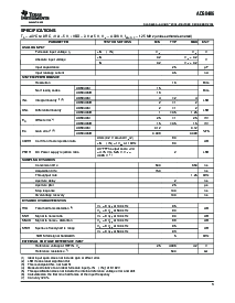
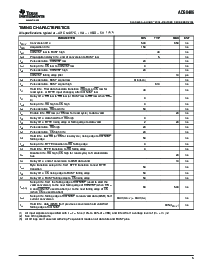
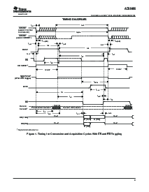
TIMINGCHARACTERISTICS
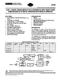
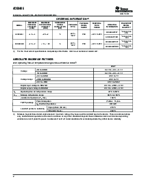
ADS8406
SLAS426A–AUGUST2004–REVISEDDECEMBER2004
Allspecificationstypicalat–40
°
Cto85
°
c,+va=+vbd=5v
(1)(2)(3)
PARAMETERMINTYPMAXUNIT
t
CONV
Conversiontime500650ns
t
ACQ
Acquisitiontime150ns
t
pd1
CONVSTlowtoBUSYhigh40ns
t
pd2
propagationdelaytime,endofconversiontobusylow5ns
t
w1
pulseduration,convstlow20ns
t
su1
setuptime,cslowtoconvstlow0ns
t
w2
pulseduration,convsthigh20ns
CONVSTfallingedgejitter10ps
t
w3
pulseduration,busysignallowmin(t
ACQ
)ns
t
w4
pulseduration,busysignalhigh610ns
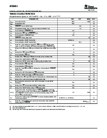
holdtime,firstdatabusdatatransition(rdlow,orcslowfor
t
h1
40ns
readcycle,orbyteinputchanges)afterconvstlow
delaytime,cslowtordlow(orbusylowtordlowwhencs=
t
d1
0ns
0)
t
su2
setuptime,rdhightocshigh0ns
t
w5
pulseduration,rdlowtime50ns
t
en
enabletime,rdlow(orcslowforreadcycle)todatavalid20ns
t
d2
delaytime,dataholdfromrdhigh0ns
t
d3
delaytime,byterisingedgeorfallingedgetodatavalid220ns
t
w6
pulseduration,rdhigh20ns
t
w7
pulseduration,cshightime20ns
holdtime,lastrd(orcsforreadcycle)risingedgetoconvst
t
h2
50ns
fallingedge
t
su3
setuptime,bytetransitiontordfallingedge0ns
t
h3
holdtime,bytetransitiontordfallingedge0ns
disabletime,rdhigh(cshighforreadcycle)to3-stateddata
t
dis
20ns
总线
t
d5
delaytime,endofconversiontomsbdatavalid10ns
bytetransitionsetuptime,frombytetransitiontonextbyte
t
su4
50ns
转变
t
d6
delaytime,csrisingedgetobusyfallingedge50ns
t
d7
delaytime,busyfallingedgetocsrisingedge50ns
setuptime,fromthefallingedgeofconvst(usedtostartthe
validconversion)tothenextfallingedgeofconvst(whencs=
t
su(ab)
60500ns
0andconvstusedtoabort)ortothenextfallingedgeofcs
(whencsisusedtoabort)
setuptime,fallingedgeofconvsttoreadvaliddata(msb)从
t
su5
最大值(t
CONV
)+max(t
d5
)ns
currentconversion
holdtime,数据(msb)frompreviousconversionholdvalidfrom
t
h4
最小值(t
CONV
)ns
fallingedgeofCONVST
(1)allinputsignalsarespecifiedwitht
r
=t
f
=5ns(10%to90%of+vbd)andtimedfromavoltagelevelof(v
IL
+V
IH
)/2.
(2)seetimingdiagrams.
(3)alltimingsaremeasuredwith20-pfequivalentloadsonalldatabitsandbusypins.
5